biolife logo
  • Home
  • Circuito Integrado
  • Componente Eletronico
  • Controle Eletrônico
  • Sobre nós
  • Política de Privacidade
  • Home
  • Know Your IC: 555 Timers

Know Your IC: 555 Timers

Circuito Integrado / December 27,2022Posted By: Gustavo Rodrigues Cavalcanti

An Introduction About IC 555 Timer, Its Features and Appliations

An IC 555 timer is one of the most flexible linear integrated circuits, which was first developed in the year 1970 by “Signetic Corporation” and named as SE/NE 555 timer. This integrated circuit is a monolithic timing circuit, which is capable of generating a precise and extremely stable time delay. Similar to other generally used operational amplifiers, this IC is also very much consistent, easy to utilize, and low cost.

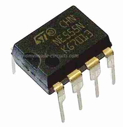
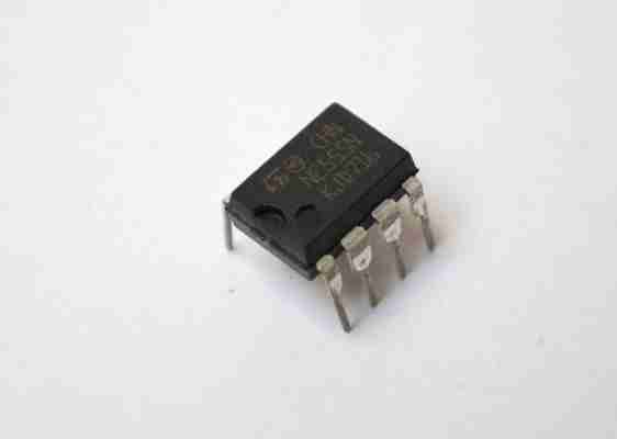
This is available in two packages an 8-pin DIP (dual in a package) and 14-pin DIP and it comprises 2-diodes, 23-transistors, and 16-resistors.

This IC is still in extensive use due to its low worth, simple to use, and constancy. It is now designed by many manufacturers in the unique bipolar & also in low-power CMOS types. As of in the year 2003, it was projected that one billion units are designed every year. This IC is the most standard integrated circuit ever manufactured.

The IC 555 timer circuit is mainly applicable in astable multivibrators, monostable multivibrators, DC-DC converters, waveform generators, digital logic probes, tachometers, analog frequency meters, temperature measurement devices, control devices, and voltage regulators. Basically the IC 555 timer works in one of these two modes: an astable multivibrator or as a monostable multivibrator. The SE555 IC is designed to operate in this range of temperature: 55°C – 125° while the NE 555 IC works over this temperature range: 0° -70°C.

The Features of the IC 555 Timer include the following

These ICs operate in a broad range of supply voltages ranging from + 5 V to + 18 V.

They Reduce or supply 200 mA of load current

The maximum power dissipation is 600 mW.

The operating temperature is 0 to 75 °C

The exterior components are chosen accurately so that the time intervals can be made in quite a few minutes along with the frequencies above several hundred kHz.

The o/p of an IC 555 timer IC can drive a TTL (transistor-transistor logic) due to its high current o/p.

The duty cycle of the 555 timers is variable.

The max power dissipation for each package is 600 mW and its two inputs like a trigger and reset have logic compatibility.

What is a 555 Timer IC?

Please refer to this link to know more about 555 Timer

555 Timer Pin Configuration

Please refer to this link to know more about 555 timer IC pin configuration

Functional Parts of the 555 Timer IC

The 555 timer IC includes three functional parts like Comparator, Voltage divider and Flip/Flop

Operating Modes of 555 Timer

The 555 timer IC has basically three operating modes such as Astable mode, Bistable Mode and

555 Timer in Monostable Mode

In this mode, the IC generates only a single pulse when the timer obtains a signal from the trigger input button. The period of the pulse depends upon the resistor and capacitor values.

555 Timer in Astable Mode

In this mode, the IC generates the nonstop pulses with the exact frequency that depends on the values of the two resistors and capacitors.

555 Timer in Bistable Mode

In this mode, the IC generates two stable states such as high and low. The output signals of these two states are forbidden by a trigger and reset input pins, not by the charging & discharging of capacitors.

Applications of 555 Timer IC

The 555 timer IC is completely used to build different electronic circuits like flashing LED, police siren, music box, LED dice, metal detector, traffic lights, etc.

Courtesy of:

IC 555 Pinout Working with Formulas

The post explains the how IC 555 works, its basic pinout details and how to configure the IC in its standard or popular astable, bistable, and monostable circuit modes. The post also details the various formulas for calculating the IC 555 parameters.

Introduction

Our hobby world would be less interesting without IC 555. It would be one of our first IC to use in electronics. In this article we are going to look back at history of IC555, their 3 operating modes and some of their specifications.

IC 555 was introduced in 1971 by a company called “Signetics”; it was designed by Hans R. Camenzind. It is estimated that about 1 billion IC 555s are manufactured every year. That’s one IC 555 for every 7 people in the world.

The Signetics Company is owned by Philips Semiconductor. If we look at the internal block diagram of IC 555 we find three 5K ohm resistors connected in series for deciding the timing factor, so probably that's how the device got its name IC 555 timer. However, some hypothesis claims that the selection of the name has no relation to the internal components of the IC, it was arbitrarily selected.

How IC 555 Works

A standard IC555 consist of 25 transistors, 15 resistors and 2 diodes integrated on a silicon die. There are two versions of the IC available namely military and civilian grade 555 timer.

The NE555 is a civilian grade IC and has operating temperature range of 0 to +70 degree Celsius. The SE555 is military grade IC and has operating temperature range of -55 to +125 degree Celsius.

You will also find the CMOS version of timer known as 7555 and TLC555; these consume less power compared to standard 555 and operate less than 5V.

CMOS version timers consist of MOSFETs rather than bipolar transistor, which is efficient and consume less power.

IC 555 Pinout and Working Details:

Pin 1: Ground or 0V: It's the negative supply pin of the IC Pin 2: Trigger or input: A negative momentary trigger on this input pin causes the output pin3 to go HIGH. This happens by a quick discharging of the timing capacitor below the lower threshold level of 1/3rd supply voltage. The capacitor then slowly charges via the timing resistor, and when it rises above 2/3rd supply level, pin3 become LOW again. This ON/OFF switching is done by an internal FLIP-FLOP stage. Pin 3: Output: It's the output which responds to the input pins either by going high or low, or by oscillating ON/OFF Pin 4: Reset: It's the reset pin which is always connected to the positive supply for normal working of the IC. When grounded momentarily resets the IC output to its initial position, and if permanently connected to ground keeps the IC operations disabled. Pin 5: Control: An external variable DC potential can be applied on this pin to control or modulate the pin3 pulse width, and generate a controlled PWM. Pin 6: Threshold: This is the threshold pin which causes the output to go LOW (0V) as soon as the timing capacitor charge reaches the upper threshold of 2/3rd supply voltage. Pin 7: Discharge: This is the discharge pin controlled by the internal flip flop, which forces the timing capacitor to discharge as soon as it has reached the 2/3rd supply voltage threshold level. Pin 8: Vcc: It's the positive supply input between 5 V and 15 V.

3 Modes of timer:

Bistable or Schmitt trigger Monostable or one shot Astable

Bistable Mode:

When the IC555 is configured in bistable mode it works as a basic flip-flop. In other words when the input trigger is given, it toggles the output stateON or OFF.

Normally #pin2 and #pin4 are connected to pull-up resistors in this mode of operation.

When the #pin2 is grounded for short duration, the output at #pin3 goes high; to reset the output, #pin4 is momentarily shorted to ground, and then the output goes low.

There is no need for a timing capacitor here, but connecting a capacitor (0.01uF to 0.1uF) across #pin5 and ground is recommended. #pin7 and #pin6 can be left unconnected in this configuration.

Here is a simple bistable circuit:

When the set button is depressed the output goes high and when reset button is depressed the output goes to low state. R1 and R2 may be 10k ohm, the capacitor may be anywhere between the specified value.

Monostable Mode:

Another useful application of the IC 555 timer is in the form of a one-shot or monostable multivibrator circuit, as shown in the figure below.

As soon as the input trigger signal becomes negative, the one-shot mode is activated, causing the output pin 3 to go high at the Vcc level. The time period of the output high condition can be calculated suing the formula:

T high = 1.1 R A C

As seen in the figure, the negative edge of the input forces the comparator 2 to toggle the flip-flop. This action causes the output at pin 3 to go high.

Actually in this process the capacitor C is charged toward VCC via the resistor RA. While the capacitor charges, the output is held high at the Vcc level.

Video Demo

When the voltage across the capacitor acquires the threshold level of 2VCC/3, comparator 1 triggers the flip-flop, forcing the output to change state and go low.

This subsequently turns the discharge low, causing the capacitor to discharge and maintain at around 0 V until the next input trigger.

The figure above shows the entire procedure when the input is triggered low, leading to an output waveform for a monostable one shot action of the IC 555.

The timing of the output for this mode can range from microseconds to many seconds, allowing this operation to become ideally useful for a range of different applications.

Simplified Explanation for the Newbies

Monostable or one-shot pulse generators are widely used in many electronic applications, where a circuit needs to be switched ON for pre-determined time after a trigger. The output pulse width at #pin3 can be determined by using this simple formula:

T = 1.1RC

Where

T is the time in Seconds

R is resistance in ohm

C is capacitance in farads

The output pulse falls when the voltage across the capacitor equals to 2/3 of the Vcc. The input trigger between two pulses must be greater than RC time constant.

Here is a simple Monostable circuit:

Solving a Practical Monostable Application

Find out the period of the output waveform for the circuit example shown below when it is triggered by a negative edge pulse.

Solution:

T high = 1.1 R A C = 1.1(7.5 x 10³)(0.1 x 10⁻⁶) = 0.825 ms

How Astable Mode Works:

Referring to the IC555 astable circuit figure below, the Capacitor C is charged towards VCC level through the two resistors R A and R B . The capacitor is charged until it reaches above 2VCC/3. This voltage becomes the threshold voltage on pin 6 of the IC. This voltage operates comparator 1 to trigger the flip-flop, which causes the output at pin 3 to become low.

Along with this, the discharge transistor is switched ON, resulting in the pin 7 output discharging the capacitor via resistor RB.

This causes the voltage inside the capacitor to fall until finally it drops below the trigger level (VCC/3). This action instantly triggers the flip flop stage of the IC, causing the output of the IC to go become high, turning OFF the discharge transistor. This yet again enables the capacitor to get charged via resistors RA and RB toward VCC.

The time intervals which is responsible for turning the output high and low can be calculated using the relations

T high ≈ 0.7(R A + R B )C

T low ≈ 0.7 R B C

The total period is

T = period = T high + T low

Video Tutorial

Simplified Explanation for the Newbies

This is the most commonly used multivibrator or AMV designs such as in oscillators, sirens, alarms, flashers etc, and this would be one of our first circuit implemented for IC 555 as a hobbyist (remember alternate blinker LED?).

When IC555 configured as astable multivibrator, it gives out continuous rectangular shaped pulses at #pin3.

The frequency and pulse width can be regulated by R1, R2 and C1.The R1 is connected between Vcc and discharge #pin7, R2 is connected between #pin7 and #pin2 and also #pin6. The #pin6 and #pin2 are shorted.

The capacitor is connected between #pin2 and ground.

The frequency for Astable multivibrator can be Calculated by using this formula:

F = 1.44/[(R1+R2*2)*C1]

Where,

F is the frequency in Hertz

R1 and R2 is resistors in ohms

C1 is capacitor in farads.

The high time for each pulse given by:

High= 0.693(R1+R2)*C

Low time is given by:

Low= 0.693*R2*C

All ‘R’ is in ohms and ‘C’ is in Farads.

Here is a basic astable multivibrator circuit:

For 555 IC timers with bipolar transistors, R1 with low value must be avoided so that the output stays saturated near ground voltage during discharge process, else the ‘low time’ could be unreliable and we may see greater values for low time practically than calculated value.

Solving an Astable Example Problem

In the following figure find the frequency of the IC 555 and draw the output waveform results.

Solution:

Waveform images can be seen below:

IC 555 PWM Circuit using Diodes

If you want the output less than 50% duty cycle shorter high time and longer low time, a diode can be connected across R2 with cathode on the capacitor side. It's also called the PWM mode for the 555 IC timer.

You can also design a 555 PWM circuit with variable duty cycle two diodes as shown in the above figure.

The PWM IC 555 circuit using two diodes is basically an astable circuit where the charge and discharge timing of the capacitor C1 is bifurcated through separate channels using diodes. This modification enables the user to adjust the ON/OFF periods of the IC separately, and therefore achieve the desired PWM rate quickly.

Calculating PWM

In a IC 555 circuit using two diodes, the formula for calculating the PWM rate can be achieved using the following formula:

T high ≈ 0.7(R1 + POT Resistance)C

Here, POT resistance refer to the potentiometer adjustment, and the resistance level of that particular side of the pot through which the capacitor C charges.

Let's say the pot is a 5 K pot, and it's adjusted at 60/40 level, producing resistance levels of 3 K and 2 K. Then depending on which portion of the resistance is charging the capacitor, the value could be used in the above formula.

If it's the 3 K side adjustment that is charging the capacitor, then the formula could be solved as:

T high ≈ 0.7(R1 + 3000 Ω) C

On the other hand, if it's 2 K that's on the charging side of the pot adjustment, then the formula may be solved as.

T high ≈ 0.7(R1 + 2000Ω) C

Please remember, in both cases the C will be in Farads. So you must first convert the microfarad value in your schematic into Farad, for getting a correct solution.

IC 555 Pulse Generator

This IC 555 circuit might seem recognizable to a lot of visitors because it is among the several versions of circuits from the common 555 timer circuits.

That does not essentially reduce its usefulness though. Simply because, a flexible pulse generator having a adjustable duty cycle can be a very handy equipment for any electronic workshop.

In contrast to the conventional 555 astable circuits that are generally implemented, the resistors between pins 6 and 7 includes P1, P2, R2, DI and D2.

A tightly characterized charging time for capacitor C1 is established by the diodes D1 and D2.

This typically results in the duty cycle of around 50%, if it weren't for P2. For the present scenario the duty cycle is determined by the relationship between P1 and P2: n = 1 + P2/P1. For instance, if P2 = 0 (n = 100%), the frequency will then be:

f = 0.69 / [2(P1+P2+4.7kΩ)C1

References: Stackexchange

Know Your IC: 555 Timers

Hello everyone

I want to make a circuit using astable mode of 555 ic in which

1. I need to generate Biphasic or Bipolar pulses at particular Frequency like 500hz

2. I want to control current between 10uA to 100uA

currently 555 ic in astable mode giving mopolar pulses (0 to +5 v ) but i want to generate +5 to -5v

Kindly guide me about this

Tags:
  • IC 555
Christian DoeGustavo Rodrigues Cavalcanti
Share:

Comments

success!!!
Failed!!!

Sidebar ×

Categories

  • Circuito Integrado (90)
  • Componente Eletronico (69)
  • Controle Eletrônico (92)

Principais artigos

  • O que são circuitos integ...

    December 01,2021

  • O Que São Circuitos Integ...

    November 28,2021

  • Circuito integrado tridimensio...

    November 29,2021

O último artigo

  • BLOG MASTERWALKER SHOP

    November 25,2021

  • Os circuitos integrados s...

    November 26,2021

  • CI circuito integrado cla...

    November 23,2021

Artigo favorito

  • Transistor: o que é, funç...

    November 22,2021

  • Circuitos integrados: o q...

    November 19,2021

  • O que são circuitos inte...

    November 16,2021

biolife logo

Principais artigos

  • O que são circuitos integ...
  • O Que São Circuitos Integ...
  • Circuito integrado tridimensio...

O último artigo

  • BLOG MASTERWALKER SHOP
  • Os circuitos integrados s...
  • CI circuito integrado cla...

Artigo favorito

  • Transistor: o que é, funç...
  • Circuitos integrados: o q...
  • O que são circuitos inte...

Copyright © 2023 snowcommunication.com. All rights reserved.